Interrupt Project Update 10-5-25
Hey everyone,
Development has been moving steadily as we refine the final pieces of the hardware. We’ve hit a few small delays as we finalize component selections and schematic details, but the team is working hard to wrap up the board design and move into layout. The extra work we’re putting in now helps ensure the device performs reliably and meets the quality you expect. We’re incredibly thankful for your continued support and encouragement. Your patience and enthusiasm keep us motivated as we bring this project closer to the finish line.
RF architecture & antenna plan:
- Matching networks and filters will sit between the selected RF switches.
- Multiple RF paths are being created for band coverage; an older approach was dropped due to obsolescence.
- Current approach: multiple internally mounted antennas (no external SMA). This balances bandwidth, simplicity, and cost.
- UI will let users select frequency bands; firmware will enable the right matching path automatically.
I/O & Audio:
- Likely adding an I/O expander to preserve standard MCU/SoC pins for core features.
- Audio options (under evaluation):
- Note: depending on audio implementation, certain buses are shared, so we are evaluating work arounds with brief UI refresh limits if audio capture is active.
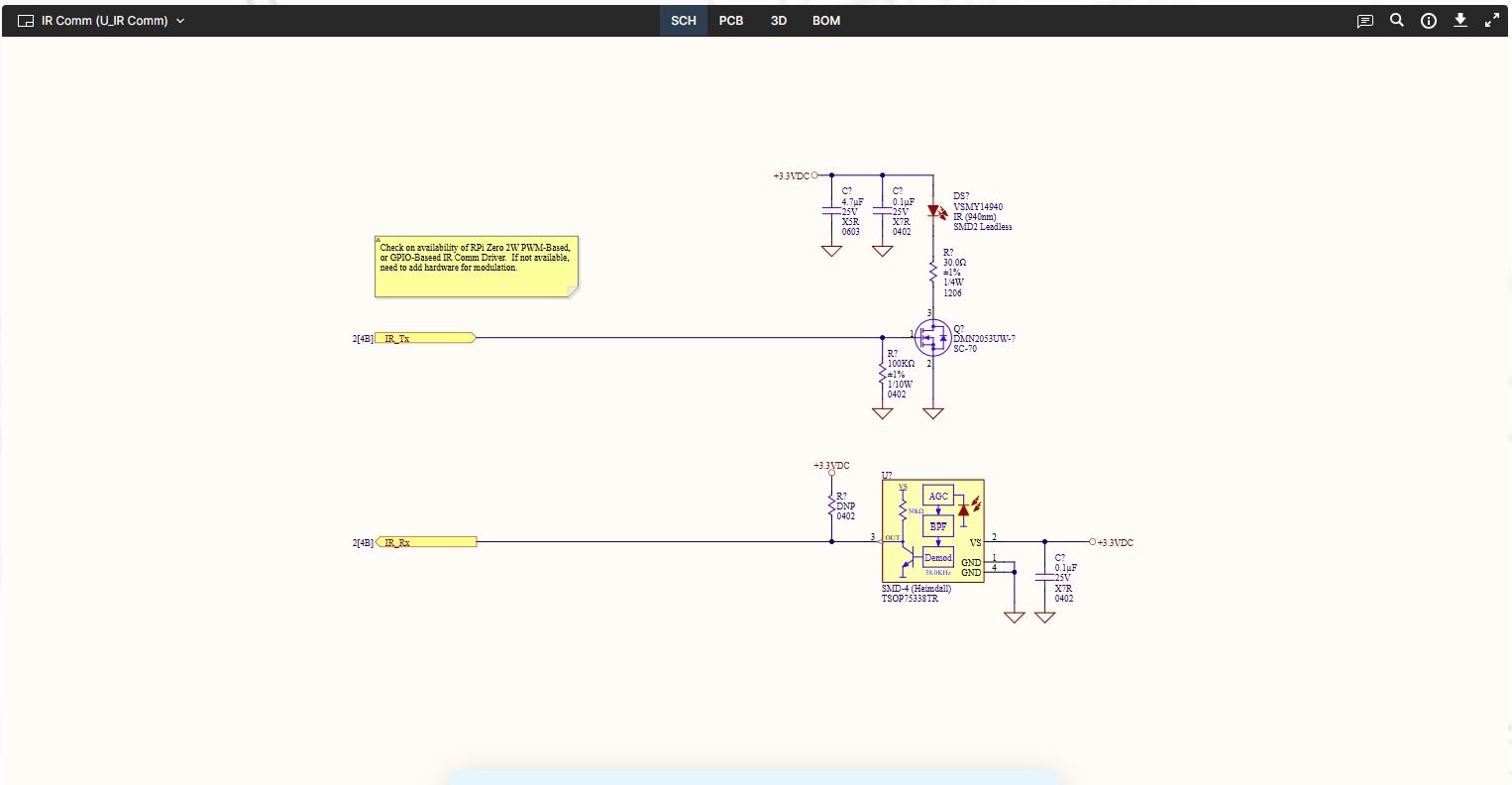
NFC & IR:
- NFC circuitry is complete pending power rail finalization and antenna tuning; goal is full capability.
- IR uses a single high-power emitter (replacing the two-emitter approach in early prototypes).
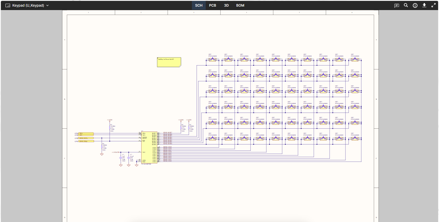
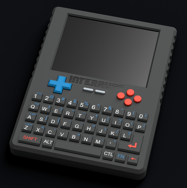
Firmware & UX:
- Display and keyboard firmware is underway on dev boards with milestone-based reviews.
- This lets us validate chunks of functionality while parallel work continues on other modules and GUI.
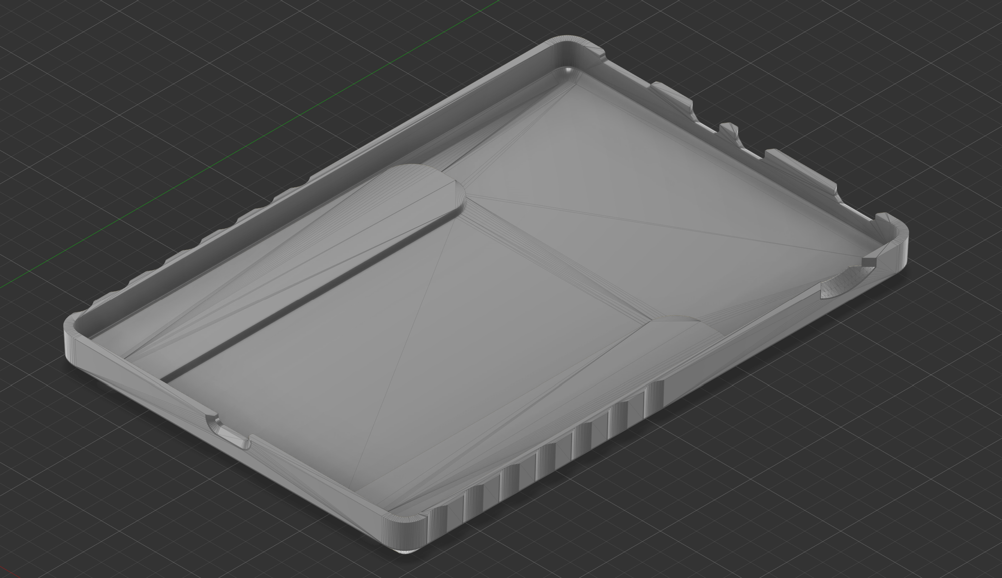
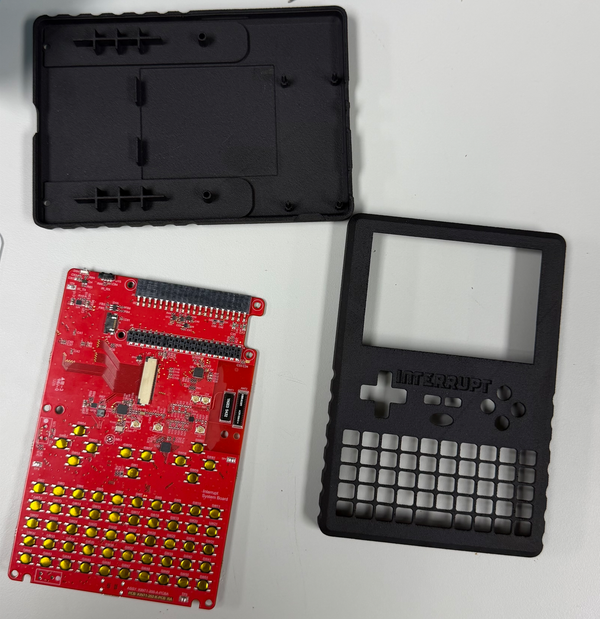
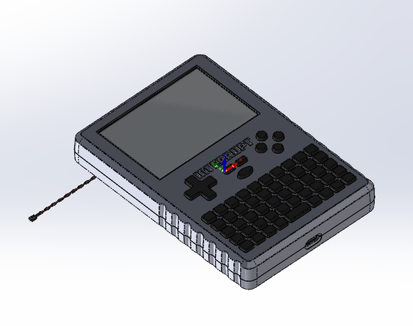
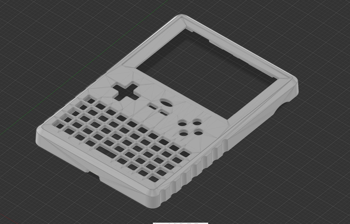
Enclosure & mechanical:
- Keep screw mounts so users can open the device for tinkering.
- Add accessible GPIO; confirm final screen-connector location during PCB placement.
- Dedicated soft-power button retained (cleaner user experience vs. multi-button combo).
- Enclosure is prototype-ready; final tweaks will follow PCB placement.
PCB & connectors:
- Board-to-connector geometry is driving a neat internal stack; extra height is negligible.
- Pi/host board mounts through the main connector for sturdiness.
What’s next:
- Finalize power schematic after confirming all peripheral loads.
- Complete RF matching/filter networks and antenna tuning parameters.
- Begin drafting FCC test plan and pre-compliance strategy.
Note: We have attached the latest enclosure STL's on our blog and discord server.